
While ASML the only company on the planet that makes the ultra-advanced lithography machines essential for every modern chip has been forced by export controls to severely restrict sales to China, it has now chosen India as a long-term strategic partner, quietly ushering the country into one of the world’s most exclusive and tightly guarded technology clubs.
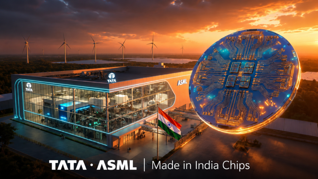
In a high-profile ceremony in The Hague on May 16, 2026, Prime Minister Narendra Modi and Dutch Prime Minister Rob Jetten witnessed Tata Electronics and ASML sign a landmark Memorandum of Understanding (MoU). The partnership will power India’s first major commercial 300mm semiconductor fabrication plant in Dholera, Gujarat a $11 billion project that marks the country’s most decisive step yet toward chip self-reliance.
Tata Electronics’ Dholera fab will produce up to 50,000 wafers per month at mature-to-mid-range nodes (28nm to 110nm), targeting high-volume applications in automotive electronics, mobile devices, AI infrastructure, power management, and industrial systems. First commercial “Made in India” chips are targeted for late 2026, with initial production expected by December 2026.
ASML, the world’s undisputed leader in advanced lithography equipment, will supply its holistic suite of Deep Ultraviolet (DUV) precision lithography tools tailored for these mid-range nodes and provide end-to-end support for fab ramp-up, process optimisation, talent development, and supply-chain resilience. Tata is also partnering with Taiwan’s Powerchip Semiconductor Manufacturing Corporation (PSMC) for process technology. The Indian government is backing the project with up to 50% capital subsidy under the India Semiconductor Mission.
Dr. Randhir Thakur, CEO and Managing Director of Tata Electronics, said the collaboration “will ensure the timely ramp of our fab in Dholera and it will go a long way in building a strong semiconductor ecosystem in India.” ASML CEO Christophe Fouquet described the project as “extremely important,” pledging “all the support ASML can give in terms of products, technology, and people.”
How This Deal Accelerates Chip Self-Sufficiency
India currently imports over 90–95% of its semiconductors, exposing the economy to global shortages and geopolitical risks. The Dholera fab directly bridges this gap by establishing domestic front-end wafer fabrication — the most technologically demanding and capital-intensive part of the semiconductor value chain.
Key ways the partnership advances Atmanirbhar Bharat:
- Domestic manufacturing at scale: For the first time, India will produce high-volume chips on its own soil instead of relying almost entirely on assembly, testing, and packaging (ATMP/OSAT).
- Irreplaceable technology transfer: ASML’s holistic lithography solutions, combined with PSMC’s process know-how, bring world-class expertise and training to India.
- Ecosystem multiplier: The project is expected to create over 20,000 direct and indirect high-skilled jobs while catalysing local suppliers for chemicals, specialty gases, photomasks, and materials.
- Strategic resilience: It reduces import dependence in critical sectors (EVs, 5G/6G, defence, data centres) and positions India as a trusted alternative in global supply-chain diversification.
Backed by the India Semiconductor Mission, this is the foundation on which a complete domestic semiconductor cluster can be built.
The Daunting Challenges That Still Lie Ahead
While the deal is historic, industry experts are clear: the hard work of execution has only just begun. Full self-sufficiency remains a multi-year journey.
Major hurdles include:
- Talent and skills gap: India has strong chip-design talent but almost zero experienced fab operators, lithography specialists, and yield engineers. Bridging this shortfall will require massive, sustained training programmes.
- Incomplete supply-chain ecosystem: Over 90% of critical inputs (ultra-pure chemicals, gases, wafers) are still imported. Building local resilience especially given China’s dominance in critical minerals could take 5–10 years.
- Infrastructure demands: Semiconductor fabs need uninterrupted ultra-pure water, stable high-voltage power, vibration-free Class 1 cleanrooms, and stringent environmental controls. Scaling these reliably across India is a significant undertaking.
- Technology node progression: Dholera starts at mature nodes. Advancing to leading-edge processes (below 10nm) for cutting-edge AI and GPUs will demand heavy in-house R&D and continuous investment.
- Execution and capital risks: Fabs are notoriously complex and capital-intensive. Delays in yield ramp-up, cost overruns, or global market shifts could test the project’s momentum.
A Historic Step — With Sustained Momentum, India Can Win
The Tata-ASML partnership is more than a commercial agreement it is powerful validation that global technology leaders now see India as a serious semiconductor manufacturing destination. With four semiconductor plants slated for commercial production in 2026 and strong policy support under the India Semiconductor Mission, the foundation for a vibrant ecosystem is finally in place.
True self-reliance will ultimately depend on flawless execution in talent development, infrastructure, and supply-chain localisation over the next decade. If India maintains this focus, the Dholera fab could be remembered as the project that moved the country from being a consumer of chips to a credible global producer.
The journey from importer to innovator has officially begun. The world is now watching whether India can turn this historic moment into lasting industrial strength.