
India just approved a ₹1.27 lakh crore Semicon 2.0 push for its chip industry. But its flagship fab isn’t expected to make a wafer before 2028.
Ashwini Vaishnaw keeps a nail on the wall of his office with nothing hanging from it. He’s said it’s reserved for one specific thing: the first silicon wafer to come out of an Indian fab. At Semicon India 2026, the government’s flagship chip conference held in Delhi from September 17 to 19, the Union IT Minister told the audience roughly when that nail might finally get used — 2028. He made the remark during a discussion at the event, adding that India’s semiconductor industry has moved from building capacity to scaling production.
That detail says more about where India’s chip ambitions actually stand than most of the headlines from the same event, which led instead with a much bigger number: a newly approved outlay of roughly ₹1.27 lakh crore for a programme called Semicon 2.0. It’s a real commitment, not just talk. But the ₹1.27-lakh-crore story and the empty-nail story are both true at the same time, and reading only the first one gives you half the picture.
What actually got announced
Semicon India 2026 was the fifth edition of the government’s annual conference, inaugurated by Prime Minister Narendra Modi on September 17 in New Delhi and bringing together more than 600 companies from 52 countries over three days. The main business of the event was unveiling Semicon 2.0, the second phase of the India Semiconductor Mission. The Union Cabinet had already cleared the programme in July, with an outlay of about ₹1,27,500 crore, which Modi described publicly as a $13.5 billion commitment.
Where the first phase was mostly about getting individual fabs and packaging plants approved, Semicon 2.0 is built around six areas — chip design, machines and materials, fabrication facilities, advanced packaging, applied research, and talent development. The government says investment commitments of roughly ₹1 lakh crore have already come in under the new phase, expected to turn into actual capital over the next two to three years rather than immediately. Separately, US equipment maker Applied Materials committed $5 billion over ten years toward research, supplier development and workforce training in India.
The stated targets are concrete: around 200 domestic chip-design firms and roughly one lakh trained technicians and factory-floor engineers, plus six new “ChipIN” regional centres meant to widen access to chip-design tools beyond the usual hubs. Markets responded fast — shares of Kaynes Technology, Syrma SGS Technology and MosChip Technologies rose as much as 10% on the day the roadmap was unveiled.
The part everyone’s skipping
Here’s where it gets more interesting than “government announces big number.” At the same event, officials also updated the scorecard for the first phase — launched in December 2021 with a ₹76,000 crore outlay — and that scorecard is the real story.
Since 2021, the Mission has approved a dozen projects across six states, with combined investment upwards of ₹1.6 lakh crore, including the flagship Tata Electronics–PSMC wafer fab in Dholera, Gujarat, and Micron’s packaging plant in Sanand. Of those approved projects, five are now in commercial production, and Modi confirmed as much on stage. That’s genuine progress — five years ago there were none.
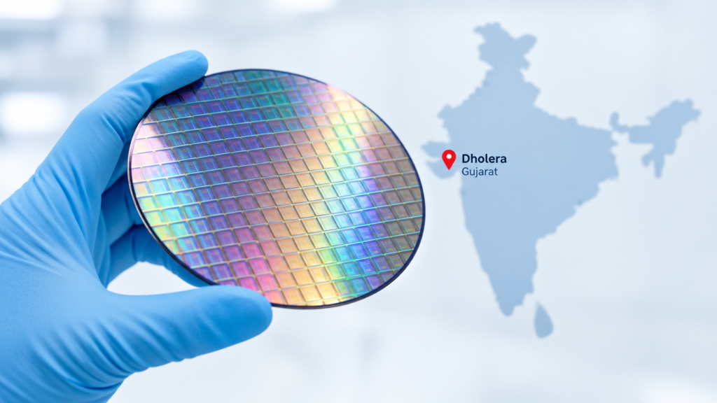
But all five running plants are what the industry calls ATMP or OSAT facilities: assembly, testing, marking and packaging. They take chips fabricated elsewhere and finish, test and package them. Not one of them turns raw silicon into a chip. That job belongs to Tata Electronics’ fab in Dholera — India’s first large commercial wafer fab, designed for up to 50,000 wafers a month, mostly at older 28nm-to-110nm nodes rather than cutting-edge ones. It’s been under construction since 2024, and Vaishnaw’s own words at the September event put its first wafer at 2028. Until that wafer exists, calling India a “chip manufacturing” nation describes an intention more than an output.
The numbers behind the noise
The gap matters because of where India’s chip demand is headed. The government’s own projection has domestic semiconductor consumption crossing $110 billion by 2030, pushed mainly by smartphones, EVs and AI-linked electronics. Against that, one recent policy analysis put India’s cumulative semiconductor import bill at close to $150 billion between FY17 and FY25, growing at roughly 23% a year — and warned that annual imports could reach $240 billion by 2035 if domestic manufacturing doesn’t scale. Every year Dholera isn’t shipping wafers is another year that gap is filled by imports rather than anything made in India. Add the two Mission phases together — ₹76,000 crore plus ₹1,27,500 crore — and the government has now committed close to ₹2.04 lakh crore in outlay, against zero domestically fabricated wafers to date. That’s not a criticism; it’s the actual scoreboard.
Why this actually matters
The design-and-talent half of Semicon 2.0 is arguably the part with the more realistic near-term payoff. Training a lakh technicians and seeding 200 design firms doesn’t require a single working fab to start showing results — India already holds a meaningful share of the world’s chip-design engineering talent, and formalising that into companies and regional centres is a lower-risk bet than waiting on Dholera’s timeline. For ordinary consumers, though, don’t expect cheaper phones or laptops any time soon: packaging plants add jobs and supply-chain depth, but the components inside your devices will keep coming from abroad until an Indian fab is actually producing chips at scale.
The skeptical read
Not everyone takes the government’s technology claims at face value. Vaishnaw has said India now has 40nm chip technology and is targeting 7nm-to-3nm capability within eight years. Industry commentators have pushed back on the framing: that’s a claim about design know-how, not about what any Indian fab can currently produce — the country’s only fab actually running today, the government-owned SCL Mohali, still fabricates at roughly 180nm, a node considered obsolete for most modern electronics. By that reading, “technology roadmap” is the more honest label for Semicon 2.0’s boldest numbers than “manufacturing plan.” That doesn’t make the plan dishonest — roadmaps describe a destination, not the current location — but it’s a narrower claim than the headlines suggest.
What’s still unresolved
Three things aren’t settled. Whether the ₹1 lakh crore in Semicon 2.0 “investment commitments” turns into disbursed capital on the stated two-to-three-year schedule is unverifiable today — commitments at this stage are typically MoUs, not signed contracts. Whether Dholera’s 2028 date holds is genuinely uncertain — fabs everywhere slip, and this is India’s first attempt at one. And it isn’t clear whether the packaging-heavy first phase pulls India further up the value chain over time, or settles into a durable assembly hub while fabrication itself stays elsewhere — more than 60% of global chip production, and close to 90% of the most advanced chips, are still made in Taiwan.
What happens next
Officials around the conference indicated more plants in the pipeline should reach commercial production through 2027, with Dholera remaining the flagship target for 2028. The real test comes after that: whether Semicon 2.0’s design and talent spending produces companies capable of designing chips that Indian fabs can actually build — closing a loop that, right now, still runs mostly through fabs and design houses outside the country.
Mantra’s Take
The number that matters here isn’t ₹1.27 lakh crore — it’s zero. That’s how many finished wafers an Indian fab has produced, roughly five years and close to ₹2 lakh crore in combined Mission outlay after this project began. That’s not a case against the ambition; building a fab from nothing, in a country with no prior fabrication base, was never going to happen on a two-year clock, and the five packaging plants now running are real progress, not just paperwork. But if Semicon 2.0 gets judged only by its funding total or by 2030 demand projections, the actual test — whether Dholera ships a real wafer by 2028, and whether the fab after it takes less than seven years to get there — will get lost in the noise. That’s the number worth watching, not the one on the press release.